When selecting a stackup for a PCB, layer count plays a significant role in determining cost, signal integrity, electromagnetic compatibility (EMC), and manufacturability.
Two-layer stackups are among the most common. While widely used in cost-sensitive and simpler designs, they come with certain limitations compared to 4-layer and higher layer count PCBs, especially regarding power distribution, signal integrity, and EMC.
This article explores the strengths and weaknesses of 2-layer PCBs, how to optimize their performance, and when transitioning to a more complex stack-up becomes necessary.
What is a 2-layer PCB stackup?
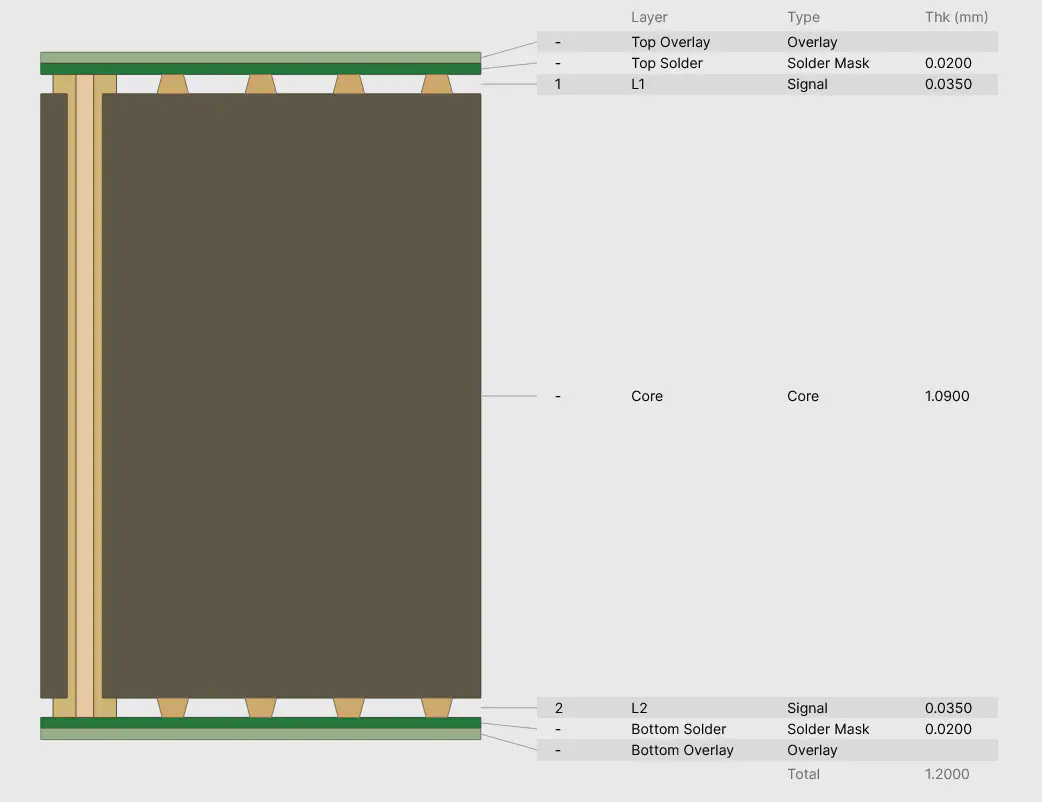
A 2-layer PCB consists of two copper layers with a dielectric material (typically FR4) sandwiched in between. Traces on both layers can be interconnected using standard through-hole vias, allowing for trace crossing and improved routing flexibility:
Unlike multi-layer PCBs that can dedicate internal planes to power and ground, 2-layer boards require careful routing to maintain electrical performance.
Advantages of a 2-layer PCB
Cost-Effective: 2-layer PCBs have lower fabrication cost compared to higher layer count PCBs, and usually they are the cheapest option available. They have a simpler manufacturing process, reducing production time and complexity.
Widely Available: 2-layer PCBs are ubiquitous. These boards are supported by virtually all manufacturers, especially if your design uses the typical 1.57mm thickness. This ensures compatibility, easier vendor switching, and faster turnaround times.
Easier Prototyping & Repair: Since all traces are accessible on the outer layers, they are easier to repair and troubleshoot. Probing, fault identification, and manual modifications are easier. Multi-layer PCBs, in contrast, have hidden internal layers that complicate rework.
These advantages make 2-layer boards ideal for quick and dirty prototyping, repairs, and DIY electronics, where easy adjustments after production are essential. They are the go-to choice for makers and hobbyists. They are also heavily supported by PCB pooling services, where multiple orders are combined into a single fabrication run, making 2-layer boards dirt cheap and accessible worldwide.
Disadvantages of a 2-layer PCB
Limited Routing Space: All component pads, traces, power, and ground must share just two layers. In contrast, in multi-layer boards, each of these categories typically get its own dedicated layers. 2-Layer boards also result in lower-density designs. If you need to add more components or traces, the board must necessarily grow to fit everything properly.
Poor Power Distribution & Grounding: Lack of dedicated power and ground planes, leading to higher voltage fluctuations and more voltage drop when high current peaks are demanded by an IC. Thicker traces are required to distribute power and ground to the components, which further reduces space and complicates routing of the rest of the signals.
Signal Integrity Challenges: Longer trace lengths and increased via usage increase resistance and inductance. Without solid reference planes, maintaining controlled impedance is difficult. This produces unpredictable impedance variations, which create reflections that especially affect high-speed signals. The limited separation between traces and the lack of a reference plane in the adjacent layer also increase signal crosstalk and noise coupling, as different signals will share the same return paths.
Poor EMC Results: Impedance mismatches and reflections also introduce high frequency noise, which is more easily radiated. Radiation is also proportional to the signal loop areas, and in a 2-layer PCB, loop areas are larger and not well defined, due to the longer traces and the lack of reference planes. This results in higher radiated emissions, as well as higher susceptibility to external noise that will be more easily coupled to your design. Without proper grounding, EMC results can also be highly unpredictable; one version of your PCB might perform well enough by luck, but minimal changes to the design might result in totally different EMC results.
Improving Signal Integrity & EMC on 2 layers
Even though 2-layer PCBs have important limitations, several techniques can be applied to enhance performance:
Use a continuous ground plane in bottom layer. This plane should be as continuous as possible, without long traces splitting it. This helps in creating a better reference and return path for the signals, and it simplifies ground connections to component pads as these can be connected to ground with just a small trace and via to the bottom layer, without long ground traces required.
Implement proper decoupling. Bypass capacitors are always important, but they are even more critical in 2-layer PCBs, as the power distribution network is worse and will usually have higher inductance. Place small-value bypass capacitors close to each power and ground pair of pins, and bigger bulk capacitors close to the ICs.
Proper power distribution. Power distribution is hard in a 2-layer PCB, but if you managed to have a continuous ground plane in the bottom layer, you’ve already done half the job. In the top layer, use power planes or traces as short and thick as possible, for routing power from the source to the bulk capacitors near the ICs.
Reduce PCB thickness. Instead of using the typical 1.6mm PCB, reducing the overall PCB thickness to 1.2mm or 1.0mm will decrease distance between the ground plane in the bottom layer and the traces and power planes in the top layer, as well as reduce via length and inductance. This will improve power distribution, reduce loop areas, which means reduced radiated emissions, and provide a better return path for signals. Avoid going below 1.0mm to maintain mechanical strength and manufacturability.
Minimize routing complexity. Try to avoid routing long traces in the bottom layer that will split the ground plane. Route most of the traces in top layer, with only small, short jumpers in bottom layer where crosses are unavoidable. Minimize trace length and layer changes. Component placement has a huge influence in this case. Arrange the components in a way that makes the layout easier and allows for more direct connections between components.
Alternative grounding techniques
While a continuous ground plane in bottom layer is still the most recommended approach, it’s not always feasible unless the design is rather simple. If you have a dense board in which you must fit many components and traces in a small area, or if you need to place components on both sides of the PCB, then you can consider applying some of these alternatives:
Copper pours with stitching vias: Fill unused areas on both layers with ground pours, and connect them with multiple stitching vias to maintain a low impedance ground network.
Ground perimeter around the PCB: Start with a ground trace in a ring shape around the PCB in both layers, connecting both with vias. Try to route all other traces within this boundary. Once you finish the design, you can then fill the empty space with a ground pour from this ring towards the center of the PCB, making it easier to keep a bigger continuous ground pour with less splits.
Grid grounding: Lay ground traces in a grid pattern, where horizontal traces are laid out in one layer and vertical traces in the other layer, connecting both together with vias at points where the grids cross. Once you start adding components and other traces, you might need to modify this grid pattern and move or delete some of the connections, but you will still have a decent grounding. After you finish the design, you would also apply a ground pour to fill the remaining empty spaces.
Though not as effective as a solid plane, these patterns can help you keep a more consistent ground reference, ensuring that different sections of the board remain at nearly the same potential, while still providing some free real estate for components in both layers. These techniques can also help you keep a guard ground around and between critical signals, to provide shielding and to allow for shorter return paths.
Case study: A well-designed 2-layer PCB
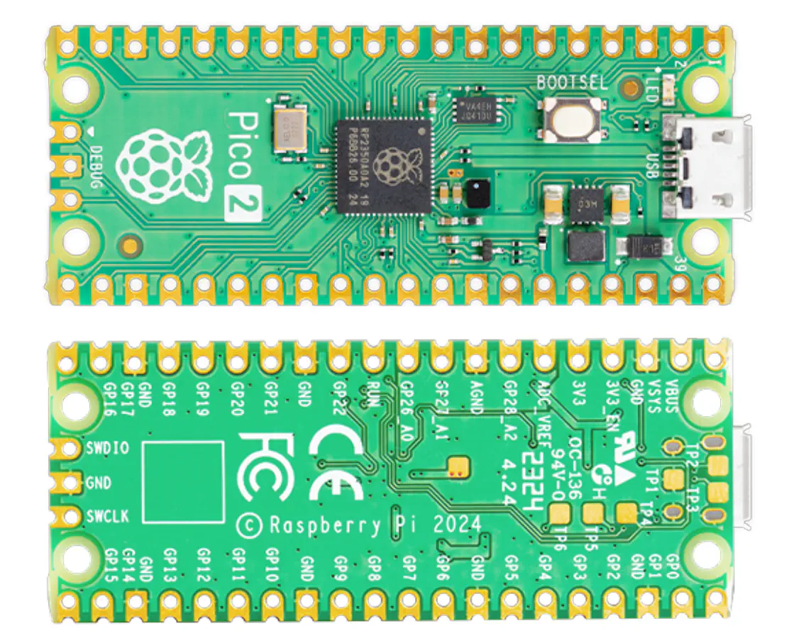
A great example of a 2-layer PCB design is the Raspberry Pi Pico family. Both the Pico and Pico 2 are high-volume, low-cost products designed to be compact and economical. These boards prioritize affordability, featuring a single-sided assembly and avoiding expensive components. In such designs, the PCB itself becomes a significant cost factor, making the use of a 2-layer PCB a practical choice.
We can see how some of the techniques we already discussed were applied:
- The bottom layer is largely dedicated to a continuous, solid ground plane, with only minimal trace interruptions where absolutely necessary.
- Traces on the bottom layer are routed carefully to minimize ground plane disruptions. Some traces even take longer paths or route through the center of the MCU to preserve uninterrupted reference planes for signals on the top layer.
- A thinner PCB is used (1.0mm instead of the typical 1.6mm), which helps reduce loop areas, improves EMC performance, and minimizes crosstalk. The reduced thickness also means less material and lower weight, making production and distribution cheaper.
- The USB 2.0 differential pair is routed directly from the MCU to the connector, maintaining controlled impedance. There are no ground plane disruptions under the pair, and the thinner PCB allows for impedance control using thinner traces, ensuring better signal integrity.
- Most other signals are also cleanly routed from the main IC to the outer pads, avoiding unnecessary crossing of traces. This direct routing was easier to achieve here, though, because they designed the IC pinout with this PCB layout in mind, a luxury not available in other designs.
- In the pads around the board, many ground pins are interspersed among GPIO pins (roughly one ground pin per four GPIOs). This minimizes loop areas and separate return paths for different signals, reducing crosstalk for the external connections.
The Raspberry Pi Pico is a good example of when a 2-layer PCB is the right balance between simplicity, cost, and performance. However, as design complexity increases, a 2-layer stackup may no longer suffice.
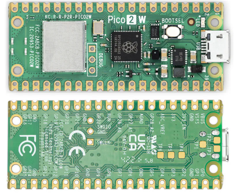
For instance, with the Pico W family, which adds Bluetooth and Wi-Fi functionality, the design transitions to a 4-layer PCB. The wireless module increases the device’s complexity and price, and introduces more stringent EMC requirements (the board is now an intentional radiator). In this case, the added cost of a 4-layer PCB is less significant and is justified by its benefits: more real estate for routing, better ground planes that can enhance antenna performance, easier EMC compliance, easier impedance control for USB and antenna traces that can now be achieved with thinner traces.
When to upgrade to a 4+ layer PCB
If you’re approaching a more complex project, here are key scenarios where a 2-layer PCB is not enough, and upgrading to a 4 or more layers board makes more sense:
Routing and component density: For dense designs, 4-layer boards offer major advantages by using internal layers for power and ground planes, freeing up surface space for components and routing. Relying on a 2-layer PCB for a complex design could lead you to use dual-side assembly, which increases manufacturing costs. If this is the case, it can be cheaper to switch to 4 layers if that helps to keep all components in one side. Additionally, 2-layer designs often demand extensive manual layout optimization to maintain signal integrity, resulting in higher development time. In many cases, switching to a 4-layer PCB simplifies routing, speeds up development, and can ultimately be more cost effective project-wise despite the higher board cost.
Controlled impedance for high-speed signals: Achieving consistent controlled impedance on a 2-layer PCB is challenging in the best case, and impossible for most complex high speed interfaces. Even if theoretically possible in some cases, the high thickness and added variability in material properties makes reliable signal performance harder to guarantee. With higher layer count PCBs it is easier to ensure proper signal integrity, preventing costly troubleshooting and redesigns caused by poor performance.
EMC and cost efficiency in the long term: Using a 2-layer PCB may offer upfront cost savings, but it often leads to challenges with EMC compliance, causing costly delays, repeated testing, and design revisions. In contrast, 4-layer PCBs provide better grounding, improve signal integrity, and increase the likelihood of passing EMC tests on the first attempt. In a commercial project that will need to pass EMC certifications, the PCB cost is a minor part of the total project expense, and using 4+ layers can significantly reduce long-term costs, debugging time, and development effort while helping with reliability, smoother certification, faster time-to-market, and future scalability.